

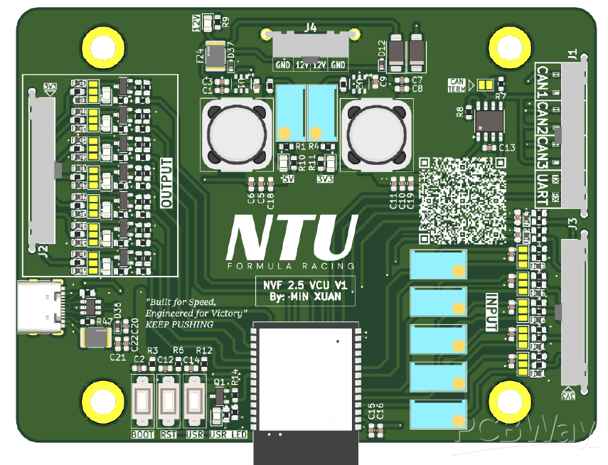
Vehicle Control Unit
The Vehicle-Control Unit (VCU) is the electronic heart of the Formula Student prototype. The board must run reliably from the car’s 12V LV Battery on track and from a laptop’s USB-C port during bench programming. This section details the microcontroller choice,
robust power tree, analogue front-end, output drivers, and high-speed interfaces.
3.2.1 Microcontroller and System Overview
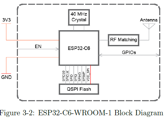
At the heart of the new Vehicle Control Unit (VCU) lies the ESP32-C6-WROOM-1-N8, a compact and highly integrated SoC module based on a single-core 160MHz RISC-V processor. Designed for connectivity-rich and embedded control applications, it offers several built-in features that simplify hardware design and accelerate development. Unlike many traditional MCUs, the ESP32-C6-WROOM-1 integrates essential system components such as a QSPI flash, a 40 MHz crystal oscillator, and an onboard RF matching network and PCB antenna, eliminating the need for external flash memory, clock crystals, or RF components. This high level of integration minimizes PCB complexity and component count. The chip supports 2 independent CAN bus controllers (TWAI—Two-Wire Automotive Interface) and includes up to 6 ADC channels via its 12-bit SAR ADC. All GPIOs on the chip are fully multiplexed and can be reassigned to various digital, analog, or communication functions via software-defined configuration, offering significant flexibility in pin planning.
Figure 3-2 illustrates the internal block diagram of the module.
3.2.2 Power Architecture
3.2.2.1 Redundant 12 V entry
The low-voltage battery feeds the board through a 4-pin Micro-Fit 3.0 header (2×power, 2×ground). Parallel pins halve contact resistance and provide fail operational redundancy if a crimp or trace opens. A 2A resettable polyfuse (F1) and a 600W bidirectional TVS diode (SMCJ58A) clamp load-dump transients to ≤ 58V.
3.2.2.2 Dual 5 V rails (VCC 5V)
Two mutually-isolated sources can energise the 5V plane: 1. Car path — The 12V line is stepped down by an ST1S3470 synchronous buck
(2 A). 2. USB path — VBUS from the host PC passes through its own 2A polyfuse and another B340A before joining VCC 5V, preventing back-feed into the laptop.
3.2.2.3 Independent 3.3 V logic rails
Two independent sources—5V USB and VCC (from the car’s 12V supply)—are routed through separate Schottky diodes into a dedicated synchronous buck regulator (distinct from the 5V converter described in Section 3.1.3.2) to generate the 3.3V logic rail:
• 12 V→3.3 V: A second ST1S3470 supplies up to 1.5A for normal in-car operation.
• 5 V→3.3 V: The same converter also accepts USB-derived 5V USB for bench-top debugging and programming when VCC is absent. When both sources are present, their respective Schottky diodes form a prioritybased OR’ing network; the higher-voltage input automatically takes precedence without requiring additional logic. Importantly, this architecture isolates the 3.3V supply from the intermediate 5V rail.
By drawing power directly from the 12V input, the design ensures that any failure in the 5V buck—whether due to overcurrent, component degradation, or backfeed—cannot compromise the stability of the MCU power domain.
3.2.2.5 Over-current and Over-voltage Protection
3.2.2.5.1 Over-current.
A primary 2A fast-acting fuse (F24) is placed immediately after the Micro-Fit 1×2 power connector, so any wiring short is cleared before energy can reach the PCB copper planes. shows PCB routing of the main fuse aforementioned. Downstream, each functional domain is isolated by self-resetting PPTC poly-fuses sized to 500mA that current-limit every sensor, digital-I/O and CAN line.
3.2.2.5.2 Over-voltage.
Load-dump and ESD transients are clamped in concentric rings of TVS devices chosen for the specific rail voltage. The 12V entry is shunted by an UCLAMP1201 TVS, rated for standoff at 14V and a 600W surge so that 40V, 400 ms ISO-16750 events are contained before the buck input. USB power and data pairs are protected by a dedicated USBLC6-2SC6 ESD array (Figure 3-10) together with an UCLAMP0501 on VBUS to survive cable-hot-plug. All logic-level nodes—including every GPIO, CANH/L and the 3.3V rail—fan out through UCLAMP3301 low capacitance TVS diodes (D9, D13, D25 etc.) that clamp at ≈5.5V, ensuring sub-nanosecond response without degrading signal. Together, the PPTC current hierarchy and rail-specific TVS network yield a layered defence that lets the VCU ride through both chronic shorts and the worst single-shot transients expected in a Formula Student electric racer.
MORE DETAILS CAN BE REQUESTED ON DEMAND :)
- Formula Student
- Vehicle Control Unit
You might like


- Comments(0)
- Likes(0)