There is no such thing as a standard printed circuit board. Each PCB has a unique function for a particular product. Therefore, producing a PCB is a complex process of many steps. This overview covers the most important steps when producing a multilayer PCB.
When you order PCBs from the PCBWay, you are buying quality that pays for itself over time. This is guaranteed through a product specification and quality control that is far more stringent than other suppliers, and ensures that the product delivers what it promises. In the production flow below you can see where the PCBWay process is unique or goes beyond the IPC standard.
Making a PCB - PCB Manufacture step by step
- 01.Pre Production Engineering
- 02.Preparing the phototools
- 03.Print inner layers
- 04.Etch inner layers
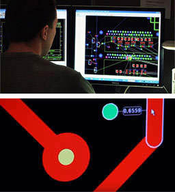
- 05.AOI
- 06.Lay-up and bond
- 07.Drilling the PCB
- 08.Electroless copper deposition
- 09.Image the outer layers
- 10.Plating
- 11.Etch outer layer
- 12.AOI
- 13.Soldermask
- 14.Surface finish
- 15.Profile
- 16.Electrical test
- 17.Final inspection
- 18.Packaging
01.PPE - Pre Production Engineering
Customer supplied data (gerber) is used to produce the manufacturing data for the specific PCB (artworks for imaging processes and drill data for drilling programs). Engineers compare demands/specifications against capabilities to ensure compliance and also determine the process steps and associated checks. No changes are allowed without PCBWay Group permission.